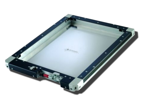
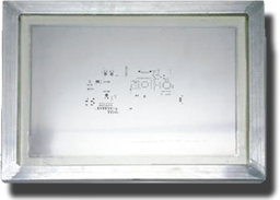
Stencil
Whats SMT stencil ?
Surface mount pcba stencils are far more than just sheet of metal, it plays a very important role in the PCBA process. The primary function of the stencil is helping to deposit the optimum amount of paste onto each individual pad of the
PCB. They are the single most important tool whose design and optimisation influences the success of every surface mount assembly line.
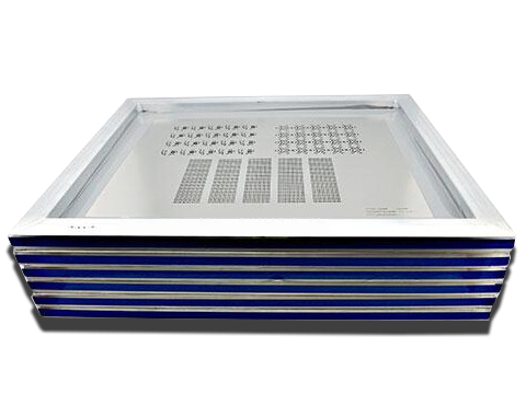
Chemical etching stencil using photo etching, is a subtractive process that selectively removes metal by chemical action. It is a cost-effective process, usually its appropriate for IC pitch larger than 60 mil, for finer pitch requirements laser cutting are recommended.
Chemical etching
Can be used for non-fine pitch printing applications
For component pitches down to 0.635mm
All apertures created simultaneously- Good paste release
Cost effective process
Durable stainless steel material
Laser cutting
For component pitches down to 0.4m
Improved aperture accuracy
Enhanced paste release
Durable full hard stainless steel material
Laser technology is ideally suited for dense, highly compacted boards with fine pitch features even down to 16mil, the photographic steps are not needed and date file is used for production directly, Using speed Lasers offers a very good accuracy and smoothest aperture walls, Far superior to Chemically etched Stencils. The opening position
tolerance could be controlled under 4m. Though laser cutting stencil is a bit more expensive, but it has superior
accuracy for 16mil fine pitch apertures.
Aperture Size
To achieve proper paste release from the stencil, an apertures aspect ratio should be >1.5, and the area ratio should be >0.66. When the stencil separates from the board, paste release encounters a competing process; solder paste
will either transfer to the pad on the board or stick to the aperture side walls. When the pad area is greater than 0.66
of the inside aperture wall area, a complete paste transfer should occur. Please see the below calculator which you
can use to determine pad size for your aperture, and foil thickness of the pcba stencil.